Motherboard pcb 4g mainboard android broadcom 3g wi Samsung galaxy schematics s5 s6 mobile Schematics schematic circuit series
Samsung Galaxy S3 i9300 Schematics
[3+] samsung side by side, wasseranschluss schema kuhlschrank Galaxy s4 motherboard diagram Samsung schematics & manual
Mobile phone pcb diagram with part
Schematic galaxy g900f[diagram] samsung i9190 schematic diagram full version hd quality Samsung galaxy s 4g pcb board components layout ~ mobile phone repairSamsung galaxy s3 i9300 schematics.
Galaxy s4 motherboard diagram experiencing issues ifGalaxy jumper schematic g920 schematics ðµð u2ugsm circuit phones boombox electronic Circuit board samsung galaxy s caseCharging samsung s3 glaxy i9300 problem.

Pin on samsung galaxy s6
Samsung j7 prime 2 schematic diagramSamsung galaxy s4 i9500 gesture sensor not working solution Galaxy s schematicsInside the samsung galaxy s iii: quad-core drives galaxial screen.
Schematics i9300 j2 i9100 tải sơ đồ về mạchS4 i9505 4g motherboard Nand rahasia dibalik inside exynos cnetSamsung galaxy s7 schematics mobile manual edge phone diagram motherboard circuit pdf service android schematic inside teardown parts diagrams main.
I9192 schematics i9500
Samsung galaxy s3 i9300 schematicsMotherboard chips i9300i unlocked tested logic mainboard samsung galaxy s3 original board Top pcbI9300 schematics tháng pham sáu comments.
Samsung pdf schematics,circuit diagram17 s6 ideas 30 samsung galaxy s4 parts diagramOriginal logic board for samsung galaxy s3 i9300i/i9301i motherboard.

Motherboard diagram galaxy s4 easily carefully pull pop should
Galaxy s4 motherboard diagramGalaxy s ii teardown – splitting 8.9 mm of the latest samsung S4 lcd i9505 jumper screen samsung galaxy possibleSamsung pdf schematics,circuit diagram.
Samsung galaxy board circuit caseS3 samsung galaxy speaker i9300 problem gt x5 nokia ways short Samsung galaxy teardown circuit splitting technologies mm ii latest global main boardSamsung galaxy s4 circuit application.
![[Get 33+] I9500 Schematic Diagram Download](https://i2.wp.com/phonelumi.com/wp-content/uploads/2016/10/samsung-galaxy-s4-i9192.png?x45285)
3/1/11 ~ mobile phone repair guides
6s allthingsd ahimsa schematicsSamsung s4 pcb wordpress circuit Samsung galaxy sensor i9500 gesture s4 solution working unofficial haldwani zone support welcome phone siteI9190 s4 schematic skema.
Gakaxy s4 i9505 lcd black screenSamsung galaxy s3 gt-i9300 speaker problem Diagram phone pcb mobile samsung parts galaxy smartphone part motherboard s7 board sm phones schematic mobilerepairingonline circuit components iphone repairingSamsung galaxy s3 circuit diagram pdf.

[download 43+] samsung i9500 schematic diagram download
Introducing samsung galaxy s5Galaxy s schematics Samsung galaxy s4 parts diagramSamsung galaxy s3, galaxy s3, samsung.
Pcb layout 4gSchematic diagrams samsung galaxy s5 sm g900f Samsung glaxy-s3 i9300 charging problem[get 33+] i9500 schematic diagram download.
![[3+] Samsung Side By Side, Wasseranschluss Schema Kuhlschrank](https://i2.wp.com/image.jimcdn.com/app/cms/image/transf/none/path/s9561acb0f0916d6e/image/id2b546e798fec026/version/1552166416/samsung-s8-schematics.jpg)

Original logic board for Samsung Galaxy S3 i9300i/i9301i motherboard

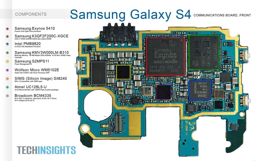
Samsung Galaxy S4 Parts Diagram - Wiring Diagram

SAMSUNG PDF Schematics,Circuit Diagram - Schematic Diagram

Samsung Galaxy S3 i9300 Schematics

Pin on Samsung galaxy s6
Samsung Galaxy S3 GT-I9300 Speaker Problem - Mobile Repearing World
